Epi lift-off wafer process
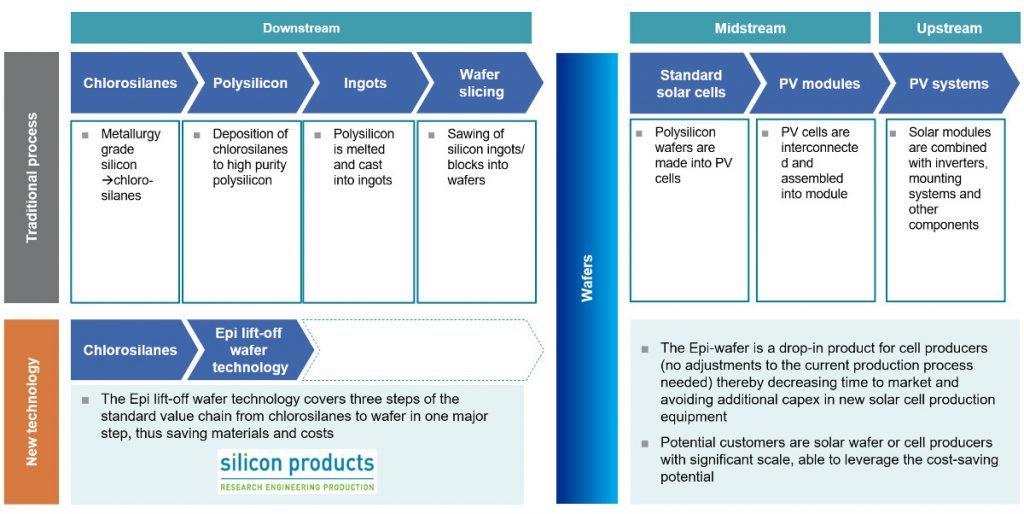
Our company is developing a new process for the production of silicon wafers. In contrast to the common state-of-the-art process for wafer production via recrystallization of poly-silicon and sawing of the ingot, the new method eliminates the loss of ingot material, known as kerfloss. The silicon wafer is processed directly from the gas phase via chemical vapor deposition of trichlorosilane.
click to the picture to enlarge

click to the picture to enlarge

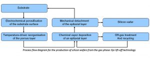
SPB aims to run this process on a high volume manufacturing scale. An overview of the individual, new process steps including the main existing unit is given in the following figure.
Epi-wafer process flow
Key benefits:
- Considerable lower production costs and high material savings compared to traditional process.
- High efficiency of 23% for n-type monocrystalline wafer.
- Production of standard full square p- or n-type monocrystalline wafers.
- High flexibility of dopant level and geometry of monocrystalline silicon wafer: full square size and variable thickness with considerable less degradation.
- No need for solar cell manufacturers to change existing production lines (“drop-in”).
Low barriers of implementation for SPB:
- Utilizing its own high-quality silicon production plant including off-gas recycling.
- Replacing the standard Siemens reactors with new high throughput fast deposition epitaxial reactors.
- Existing manufacturing track record in high quality silicon production.
- The new plant allows SPB to continue to produce FZ feed rods and hexachlorodisilane for the semiconductor industry.
Parts of the collaboration are funded by the “European Regional Development Fund” (ERDF/EFRE).
![]()